
info@universallab.org
WhatsApp: +41762172997
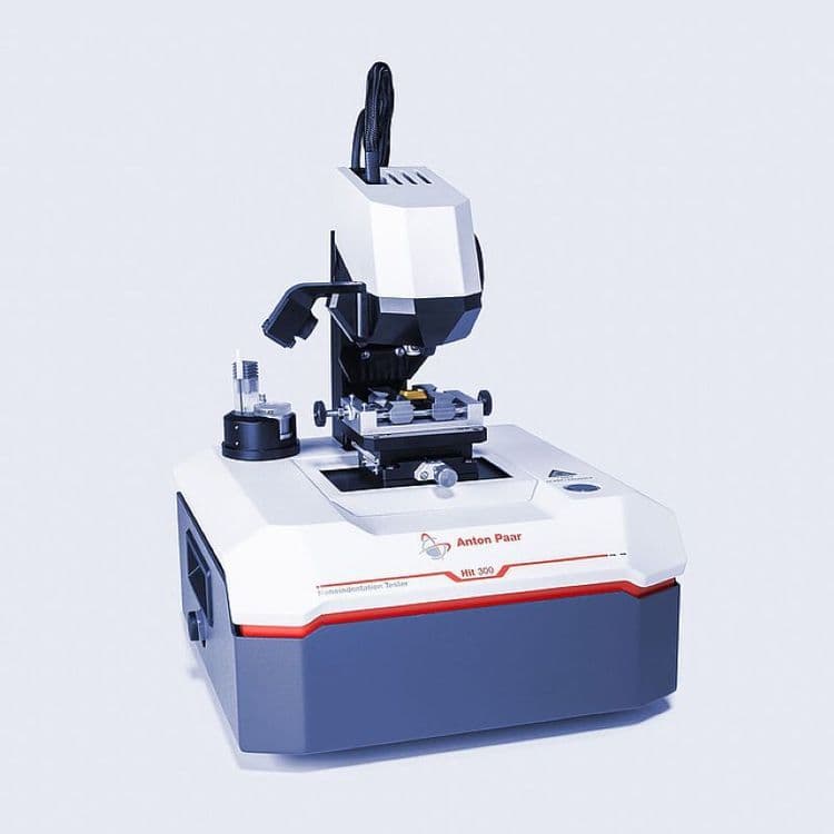
Nanoindentation
Variant (SKU)
Standard mode
CSM
DMA
Embedding and polishing
SPM+
Price may vary based on selected options
Delivery time: 1 ~ 2 weeks
Nanoindentation is a precise method for measuring the hardness and elastic modulus of materials. It applies controlled loads at the nanoscale to assess surface deformation and mechanical properties. Widely used in materials science, semiconductors, and coatings, this technique provides essential data on hardness and plasticity, supporting material development and application.

Introduction
Introduction
Nanoindentation technology is a sophisticated technique used to measure the mechanical properties of materials at the nanoscale. This method involves applying a controlled load to a sharp indenter, which penetrates the material's surface. The resulting deformation is then analyzed to determine key properties such as hardness, elastic modulus, and plasticity.
Key Features
- High Precision: Nanoindentation allows for measurements at the nanometer scale, providing detailed insights into material behavior that traditional methods cannot achieve.
- Wide Applicability: This technique is widely used across various fields, including materials science, semiconductor manufacturing, coatings, and biomaterials, making it essential for evaluating the performance of advanced materials.
- Minimal Sample Requirements: Nanoindentation requires only small amounts of material, making it ideal for testing thin films and small samples.
- Real-Time Data: The technology provides real-time data on the loading and unloading process, allowing for immediate analysis of material properties.

Principle
Principle
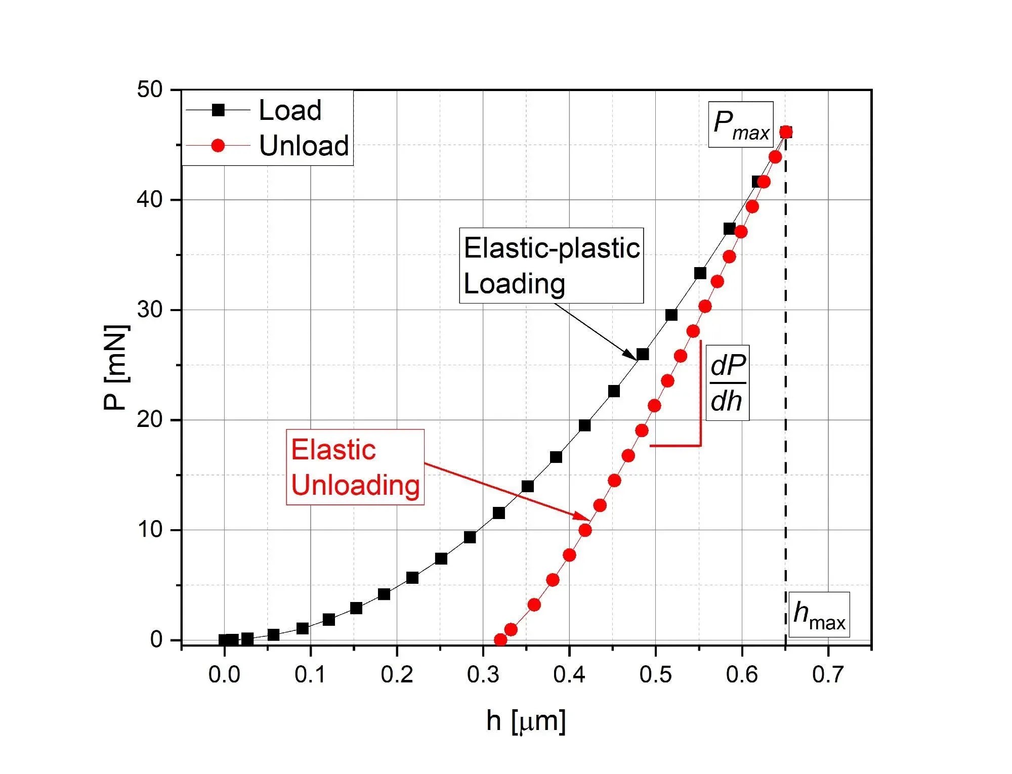
Nanoindentation is a technique for measuring the mechanical properties of materials at the nanoscale. It involves pressing a sharp diamond indenter into a sample's surface with a controlled load. As the indenter penetrates, both elastic (reversible) and plastic (permanent) deformations occur. The load and depth of penetration are continuously monitored, generating load-displacement data. This data is analyzed to determine key properties such as hardness, calculated from the maximum load divided by the contact area, and elastic modulus, derived from the unloading curve. Nanoindentation provides valuable insights into material behavior, aiding in the optimization of performance across various applications.
Sample Requirements

Technical Parameters
- Sample Size: Typically, samples should be around 10 mm × 10 mm × 1–3 mm. The surface area should be large enough to allow proper spacing between test points and avoid edge effects.
- Surface Flatness: The sample surface must be highly flat and free from significant waviness or scratches. Uneven surfaces can cause inaccuracies due to poor contact with the indenter.
- Surface Polishing: A mirror-like finish is recommended (Ra < 50 nm). Final polishing is typically done using diamond suspension (e.g., 1 µm or 0.25 µm).
- Cleaning: The surface should be free from contaminants, such as polishing residue, oil, or dust. Ultrasonic cleaning in ethanol and deionized water, followed by drying, is recommended.
- Material and Mounting: Samples must have sufficient hardness and thickness to avoid bending or substrate effects during testing. Thin or irregular samples should be mounted or embedded (e.g., in epoxy resin) for stability.
- Special Requirements: If the sample includes coatings, multilayers, or micro-scale features, please specify their thickness and structure. If you require specific loading ranges (e.g., <10 mN), test areas, or number of indentations, please indicate in advance.
Application Case

Applicable industries
Applicable materials type
- Metals & Alloys: Evaluates how microstructures like grain boundaries and precipitates affect hardness and modulus; used in advanced alloys, solder joints, and thin films.
- Ceramics: Measures fracture resistance and density in hard, brittle materials.
- BoldPolymers & Composites: Assesses mechanical properties at interfaces and phases, especially in thin films and complex structures.
- Coatings & Thin Films: Ideal for analyzing hardness, modulus, and adhesion of submicron coatings.
- Semiconductors: Used to study mechanical behavior of materials like silicon, GaN, and SiC in chips and MEMS/NEMS devices.

Industrial Application
Industrial Application
- Microelectronics & Semiconductor Industry: Used for mechanical property mapping in chip structures, packaging layers, interconnect metals, and dielectric materials.
- Aerospace: Applied to high-performance alloys and coatings, such as titanium alloys and thermal barrier coatings (TBCs), for localized property evaluation.
- Energy & Power Industry: Suitable for mechanical testing of nuclear materials, thermal barrier layers, battery films, and electrode materials.
- Automotive Industry: Used to assess lightweight alloys, composites, and key surface coatings (e.g., hardening layers, lubricating films) for wear and performance.
- Biomaterials & Medical Devices: Enables micro-scale testing of mechanical properties in dental materials, artificial bones, coated stents, and other biomedical materials.
- Academic Research & Education: Widely used in materials science, physics, chemistry, and engineering research and teaching laboratories.
Example Result
Caption: Results of the nanoindentation test.
What our customers are saying
Need precise analysis? Contact us – we'll help you choose the best solution for your needs.

Frequently Asked Questions
Nanoindentation testing technology is a high-precision method used to measure the hardness and elastic modulus of materials by applying controlled loads at the nanoscale and observing surface deformation.
It is primarily used in materials science, semiconductors, coatings, thin films, and biomaterials to assess mechanical properties.
Samples should have good surface flatness and cleanliness, sufficient thickness to avoid substrate effects, and uniform material composition.
This technology offers high sensitivity, the ability to test small samples, and provides accurate mechanical property data.
Ensure that the sample is securely fixed to avoid vibrations and temperature fluctuations that could affect the results.