Transmission Electron Microscopy (TEM) is a powerful analytical technique used to observe the microstructure of materials at the atomic or nanoscale. Unlike conventional optical microscopy, which uses visible light, TEM employs a beam of electrons that is transmitted through a thin sample. This allows for much higher resolution imaging, enabling researchers to visualize structures and defects that are not detectable with light microscopy.
TEM operates by focusing electrons onto a sample, which must be thin enough (typically less than 100 nm) for the electrons to pass through. As the electrons interact with the sample, they provide information about its morphology, crystallography, and chemical composition. The resulting images and diffraction patterns can reveal critical details about the arrangement of atoms, phases present, and the presence of defects.
This technique is widely used in various fields, including materials science, nanotechnology, semiconductor research, and biology. TEM plays a crucial role in advancing our understanding of material properties and behaviors, making it an essential tool for both academic research and industrial applications.
Principle
Principle
Transmission Electron Microscopy (TEM) uses a high-energy electron beam transmitted through a thin sample to produce high-resolution images and diffraction patterns, providing detailed information about the material's microstructure, defects, and composition.
Electron Beam Emission: The electron gun emits a high-energy electron beam, which is focused into a fine beam by the condenser lens.
Electron Beam Transmission Through the Sample: The electron beam passes through an ultrathin sample (typically less than 100 nm thick) and interacts with the atoms in the sample, including both elastic and inelastic scattering.
Sample preparation involves thinning the material to the required thickness, which can be achieved through mechanical grinding, ion beam polishing, or chemical etching. Cleanliness and proper mounting on TEM grids are also crucial.
TEM (Transmission Electron Microscopy) provides detailed information about materials at the nanoscale, including microstructural insights such as grain size and shape, phase identification, and defect characterization. It allows for crystallographic analysis, revealing lattice parameters and symmetry, as well as morphological analysis of nanostructures. Additionally, TEM facilitates chemical composition analysis through techniques like Energy Dispersive X-ray Spectroscopy (EDX) and enables interface examination between different materials. It also supports dynamic studies, allowing real-time observations of materials under varying conditions. This comprehensive information is crucial for advancing research in materials science, nanotechnology, and various industrial applications.
TEM requires samples to be extremely thin, which may not be feasible for all materials. Additionally, the technique can be sensitive to contamination and requires careful sample handling.
Applicable Material Types
Applicable Material Types:
Metals and Alloys: TEM is widely used to analyze the microstructure of metals and alloys, including grain size, phase distribution, and dislocation structures. This is crucial for understanding mechanical properties and performance.
Semiconductors: In semiconductor materials, TEM helps in examining defects, interfaces, and the crystalline structure. It is essential for the development of microelectronics and nanotechnology.
Ceramics: TEM is employed to study the microstructure of ceramics, including their crystallinity and porosity. This information is vital for applications in electronics and structural materials.
Nanomaterials: TEM is instrumental in characterizing nanomaterials, such as carbon nanotubes and nanoparticles, providing insights into their morphology, size, and distribution.
Biomaterials: In the field of biomaterials, TEM is used to investigate the interactions between biological tissues and materials, aiding in the development of medical implants and drug delivery systems.
Industries and Applications
Industries and Applications:
Electronics: TEM is crucial in the electronics industry for the development and quality control of semiconductor devices, integrated circuits, and nanostructured materials.
Materials Science: In materials science research, TEM is used to investigate the fundamental properties of materials, leading to innovations in metallurgy, polymers, and composites.
Nanotechnology: TEM plays a significant role in nanotechnology, enabling the characterization of nanoscale materials and devices, which are essential for advancements in various applications, including sensors and energy storage.
Pharmaceuticals: In the pharmaceutical industry, TEM is used to study drug formulations and delivery systems, providing insights into the morphology and stability of nanoparticles used in drug delivery.
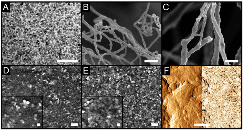
1. Caption: Material Structure and Morphology Analysis
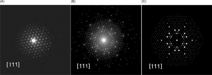
2. Caption: Crystal Structure Analysis of Materials
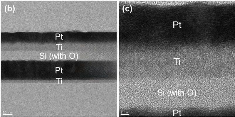
3. Caption: Interface and Surface Analysis of Materials
Technical Parameters
Sample Thickness: The ideal thickness is 30-100 nm to ensure effective electron beam transmission. For certain materials, thinner samples (around 20 nm) may be required.
Material Type: Common materials include metals (such as copper and aluminum), alloys (like stainless steel), ceramics (such as alumina), and polymers (like polystyrene). When selecting materials, consider their electron density and crystal structure.
Sample Shape: Samples should be prepared as thin sheets or films, typically circular discs with a diameter of 3 mm.For powder samples, they can be pressed into discs or coated onto TEM grids.
Preparation Methods:
Mechanical Grinding: Use 600-1200 grit sandpaper to gradually grind the sample until it approaches the desired thickness.
Ion Beam Polishing: Use an ion beam polishing machine (such as Gatan or Leica), setting appropriate voltage (usually 2-5 kV) and time to remove the final layer of material.
Chemical Etching: Use suitable chemical solutions (like hydrofluoric acid or nitric acid) for etching, controlling the etching time to avoid excessive removal.
Cleanliness: Use an ultrasonic cleaner to wash the samples, removing surface contaminants.
Operate in a dust-free environment to avoid dust and oil contamination.
Fixation and Support: Use copper or nickel TEM grids to ensure the sample is evenly distributed on the grid.
Samples can be fixed with conductive glue or resin to ensure stability during TEM observation.
Environmental Control: Prepare samples in low-temperature or inert gas environments to prevent oxidation or other chemical reactions.
Imaging Process: After interacting with the sample, some electrons transmit through it and are collected by the objective lens to form an initial image. This image is further magnified by the intermediate and projector lenses.
Image Detection: The magnified image is projected onto a fluorescent screen or a camera for observation and recording.
Aerospace and Automotive: TEM is applied in the aerospace and automotive industries to analyze materials for structural integrity, fatigue resistance, and performance under extreme conditions.
Transmission Electron Microscopy (TEM) images samples by accelerating an electron beam that penetrates thin specimens. The electron beam interacts with the atoms in the sample, resulting in scattering and transmission, which creates varying image contrasts. Ultimately, the transmitted electrons are focused by a lens system to generate high-resolution images, allowing observation of atomic-level details.