info@universallab.org
WhatsApp: +41762172997

logo-header
​
logo
Material Testing
Mechanical Testing
Tensile TestFibre Tensile TestHardness TestImpact TestFatigue TestOthers
Thermal Testing
Thermomechanical AnalysisDSCTGATGA (TG-DSC, TG-DTA)
Surface, Coating and Corrosion
Adhesion TestScratch TestCorrosion Cycle Test
Physical Properties
Functional propertiesPorosityDensity
Elemental & Chemical Composition
Compositional analysisElemental analysis
Microscopic Characterization
Particle analysisMicroscopy
Product Testing
Food & Agriculture Testing
Consumer Goods Testing
Electronics & Electrical Testing
Medical & Pharmaceutical Testing
Automotive & Transportation Testing
Packaging & Materials Testing
Chemical & Hazardous Substances Testing
Semiconductor Testing
Battery Testing
Petrochemical Testing
Environmental Test
Water Testing
Drinking Water Analysis
Soil & Sediment Testing
Soil Chemistry (pH, Nutrients)
Air Testing
Particulate Matter (PM2.5, PM10)
Noise & Acoustic Testing
Industrial/Occupational Noise
Waste & Sludge Testing
Hazardous Waste Classification
Instrumental Test
Spectroscopy
Emission
XRFXPSICP-OESGD-OES
Absorption
FTIRUV/VIS/NIRAAS
Mass Spectrometry
SIMSICP-MS
Other
RamanNMR
Microscopy
Electron
SEMTEMEBSDEMPA
Other
AFMFIB
Mechanical
Volumetric
Tensile TestFibre Tensile TestImpact TestFatigue Test
Surface
HardnessNanoindentationScratch
Others
Thermal Analysis
TGADSC
Physical Analysis
BETLaser diffractionDensityContact AngleZeta potential
Chromatography
GCHPLCIC
Services
  • Applications
  • Techniques
  • Standards
  • Industries
Regulatory testing
  • PFAS
  • REACH
  • VOC
Environmental testing
  • Water
  • Gas
Data analysis
  • XRD
  • XPS
  • FTIR
  • Raman
  • NMR
  • CT
  • SIMS
  • TGA
Blog
  • Knowledge
  • News
  • Policy
  • About us
    Contact

    Sample Requirements

    Application Case

    Example Result

    What our customers are saying

    Need precise analysis? Contact us – we'll help you choose the best solution for your needs.

    info@universallab.org+41 762172997
    Lab technician holding a blue flask

    Frequently Asked Questions

    HomeCategoryCart
    logo-footer-shop1

    European material analytical and measuring service provider dedicated for academic and industrial research

    About Us
    CareersTerms & ConditionsPrivacy Policy
    Customer Services
    Help CenterBecome a partnerReturns & Refunds
    Contact Us

    Parkstrasse 1, 5234 Villigen, Switzerland

    Email: info@universallab.org

    Phone: +41 762172997

    VAT: CHE-265.266.739 MWST

    © 2026 By Universallab. All rights reserved.

    This site is protected by reCAPTCHA and the Google Privacy Policy and Terms of Service apply.
    product
    product-0

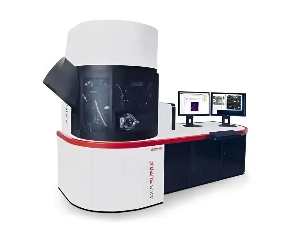
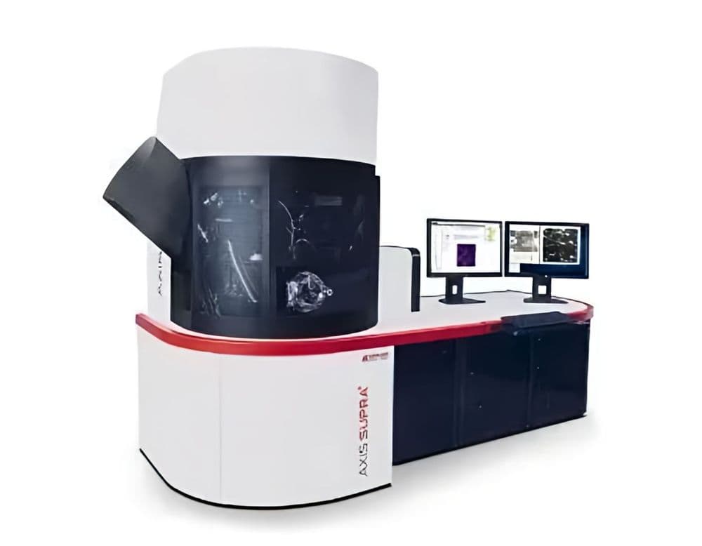
    X-Ray Photoelectron Spectrometer

    Variant (SKU)
    Survey and narrow scans
    Depth profiling
    Mapping
    Valence band only

    Price may vary based on selected options

    Delivery time: 1 ~ 2 weeks

    Introduction

    Introduction

    Introduction

    X-Ray Photoelectron Spectroscopy (XPS) is a surface-sensitive quantitative spectroscopic technique that measures the elemental composition, chemical state, and electronic state of the elements within a material. It is particularly useful for analyzing the surface chemistry of a wide range of materials.
    Advantages:

    • Surface sensitivity (probing depth of a few nanometers)
    • Provides information on elemental composition and chemical states
    • Quantitative analysis is possible

    Scope

    • Elemental Composition Analysis
    • Chemical State Analysis
    • Semi-quantitative Analysis
    • Depth Profiling
    Principle

    Principle

    Principle

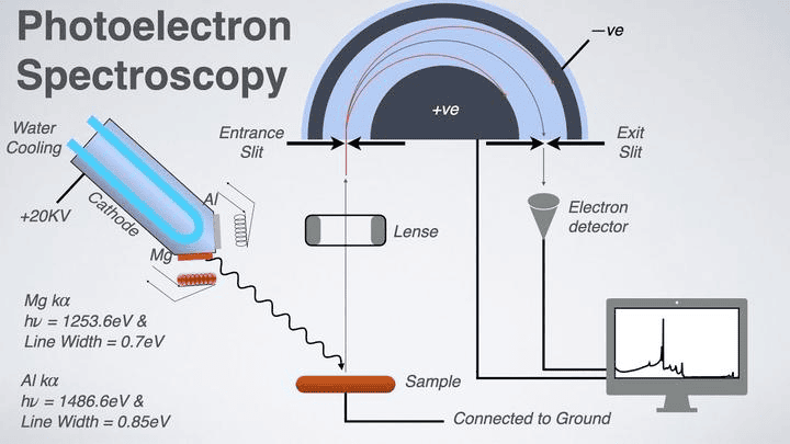
    • XPS works by irradiating a material with X-rays and measuring the kinetic energy and number of electrons that are emitted from the material's surface.These emitted electrons are called photoelectrons. By analyzing the binding energies of these photoelectrons, one can identify the elements present and their chemical state.
    • The basic principle is based on the photoelectric effect. The binding energy (BE) of an electron is related to the energy of the X-ray photon (hν) and the kinetic energy (KE) of the emitted photoelectron by the following equation: 𝐵𝐸=ℎ𝜈−𝐾𝐸−𝜙.
    • where 𝐵𝐸 is the binding energy, ℎ𝜈 is the energy of the X-ray photon, 𝐾𝐸 is the kinetic energy of the emitted electron, and 𝜙 is the spectrometer work function.

    Technical Comparison

    The following table provides a comparative overview of several commonly used techniques for elemental composition and chemical state analysis, including XPS, AES, SIMS, and EDS/EDX. The table summarizes the main information each technique can provide, analysis depth, sensitivity, quantitative capability, typical application scenarios, and spatial resolution.

    • Survey spectrum analysis is generally used to determine whether certain elements are present in a sample.
    • For samples with unknown composition, XPS survey can identify which elements are present (except H and He).
    • It is used to confirm the elemental composition of synthesized or treated samples, verifying the effectiveness of processes like doping or removal.

    XPS spectra generally include photoelectron peaks, satellite peaks, Auger electron peaks, and spin-orbit splitting (SOS), among others.

    • Photoelectron peaks: Each element has its own characteristic photoelectron lines, which are the main basis for qualitative elemental analysis. The peak with the highest intensity, narrowest width, and best symmetry in the spectrum is called the main XPS peak.
    • Satellite peaks: Conventional X-ray sources (Al/Mg Kα1,2) are not strictly monochromatic; there are also some minor satellite lines with slightly higher energy (such as Kα3,4,5 and Kβ). Therefore, in XPS, besides the main peaks excited by Kα1,2, there are also some small satellite peaks.
    • Auger electron peaks: After electron ionization, a vacancy appears in the core level. During relaxation, if another electron is excited and emitted as a free electron, this is called an Auger electron. Auger peaks always accompany XPS, but have broader and more complex structures, often appearing as groups of peaks. Feature: Their kinetic energy is independent of the incident photon energy (hν).
    • Spin-orbit splitting (SOS): Due to the coupling of an electron’s orbital and spin motion, the orbital energy level splits. For inner shells with l > 0, the spin-orbit splitting is represented by the quantum number j (j = |l ± ms|). For example, if l = 0, then j = 1/2; if l = 1, then j = 1/2 or 3/2. Except for the s subshell, all other subshells will split into two peaks.
    • Ghost peaks: Sometimes, if the X-ray source anode is impure or contaminated, the generated X-rays are not pure. The photoelectron peaks excited by X-rays from non-anode materials are called "ghost peaks."
    application

    application

    It is characterized by a small analysis area, shallow analysis depth, and non-destructive nature. XPS is widely applied in the study of various materials, including metals, inorganic materials, catalysts, polymers, coating materials, and minerals, as well as in the study of processes such as corrosion, friction, lubrication, adhesion, catalysis, coating, and oxidation.

    • Materials Science: Analyzing the composition and chemical states of materials.
    • Surface Chemistry: Studying surface oxidation, corrosion, and contamination.
    • Catalysis: Characterizing the surface of catalysts.
    • Semiconductor Industry: Analyzing thin films and interfaces.
    • Polymer Science: Studying the surface modification of polymers.

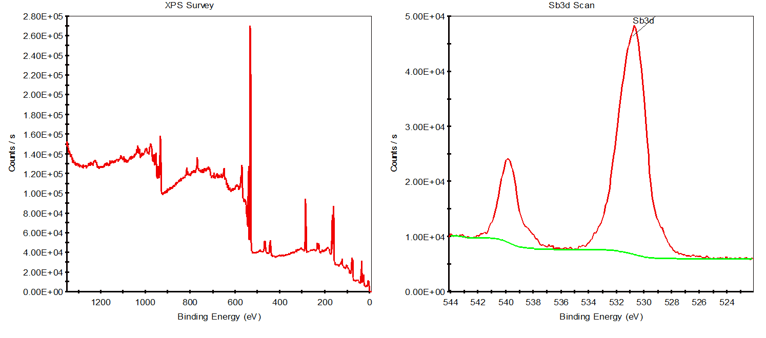
    The test results of common spectra are shown below

    The test results of common spectra are shown below

    • The survey spectrum on the left displays the binding energy distribution of all elements present on the sample surface. By analyzing the positions and intensities of these peaks, the elemental composition of the sample can be preliminarily determined, such as the presence of Sb, S, C, O, and other elements.

    • The right panel shows a high-resolution scan of the antimony (Sb) 3d region. The two main peaks correspond to the Sb 3d5/2 and Sb 3d3/2 spin-orbit components, which are characteristic features of antimony. The positions and shapes of these peaks can be used to analyze the chemical state of antimony (e.g., Sb³⁺ or Sb⁵⁺) as well as its content in the sample. The green curve represents the background subtraction, while the red curve is the actual signal.

    • XPS analysis is widely used for characterizing the surface elemental composition and chemical states of nanomaterials, organometallic complexes, thin films, and catalysts. It is commonly employed to verify the successful incorporation of target elements, changes in oxidation states, and the effectiveness of surface modifications.

    Conclusions

    X-ray Photoelectron Spectroscopy (XPS) is a powerful and widely used technique for surface analysis, providing detailed information about the elemental composition, chemical states, and electronic structure of materials within the top few nanometers. Its high surface sensitivity and ability to distinguish chemical states make it invaluable in fields such as materials science, surface chemistry, catalysis, and semiconductor research.

    • The solid/thin film sample should have an area of < 1.0 cm² (less than 8x8mm), a height (thickness) of no more than 1.0mm, a thickness of 6mm, and a flat surface. The X-ray probing depth is 1-10nm.
    • Powder solid sample 10-100mg
    • The samples are required to be vacuum-dried and free from corrosive, volatile, magnetic, and radioactive substances
    • Please indicate the storage conditions of the samples (conventional, dry, frozen, refrigerated, protected from light or others)
    • Note: XPS data analysis can get the valence state and semi-quantitative data of elements. Elements with an atomic percent content of less than 5% may not detect a significant signal.
    • Note: One position is tested per sample. If multiple positions need to be tested, they will be charged as multiple samples. For thin films, bulk samples, and similar materials, if the surface composition is not uniform, it may lead to differences in the test results.
    TechniqueMain Information ProvidedDetection DepthLateral ResolutionSensitivityQuantitative AnalysisTypical ApplicationsLimitations
    XPSElemental composition, chemical state1–10 nm (surface)~10–100 μm0.1–1 at%YesSurface chemistry, thin films, polymersRequires UHV, limited to surface, slow scan

    TechniqueMain Information ProvidedDetection DepthLateral ResolutionSensitivityQuantitative AnalysisTypical ApplicationsLimitations
    XPSElemental composition, chemical state1–10 nm (surface)~10–100 μm0.1–1 at%YesSurface chemistry, thin films, polymersRequires UHV, limited to surface, slow scan
    AESElemental composition, chemical state1–5 nm (surface)~10 nm0.1–1 at%YesThin films, micro-area analysisRequires UHV, less sensitive to light elements
    SIMSElemental/isotopic composition, depth profileless than1 nm (surface), depth profiling~50 nm–1 μmppm–ppbSemi-quantitativeTrace analysis, depth profilingMatrix effects, complex quantification
    EDS/EDXElemental composition~1 μm (bulk/surface)~1 μm~0.1 wt%Semi-quantitativeBulk analysis, inclusions, mappingPoor for light elements, lower surface sensitivity

    Test procedure

    • Sample Preparation: Samples need to be clean and representative of the material being studied.
    • Vacuum Conditions: The analysis is performed under ultra-high vacuum (UHV) conditions to minimize contamination and allow the photoelectrons to reach the detector without scattering.
    • X-ray Irradiation: The sample is irradiated with a beam of X-rays.
    • Electron Detection: Emitted photoelectrons are collected and analyzed by an electron spectrometer, which measures their kinetic energy.
    • Data Analysis: The resulting spectrum (a plot of electron intensity versus binding energy) is analyzed to identify elements and their chemical states.

    • The survey scan is mainly used for qualitative analysis, and its parameter step size is relatively large, so elements with low content may not show peaks in the survey scan.
    • If a peak appears in the high-resolution scan, it indicates the presence of that element.

    No, it is not. The sensitivity factor of the main peak is different for each element.

    You should look at the magnitude of the residuals—the smaller, the better. You also need to consider the physical meaning of the fit. The number of peaks to fit depends on the actual situation of the sample and the degree of fit; there is no strict rule as to which is better.

    XPS (X-Ray Photoelectron Spectroscopy) is a technique that measures the energy distribution of photoelectrons emitted from a sample surface under X-ray irradiation. It enables qualitative and semi-quantitative analysis of surface elemental composition, chemical states, and molecular structure. XPS is widely used in materials science, surface chemistry, and semiconductor research for its high surface sensitivity and ability to provide detailed chemical information.