info@universallab.org
WhatsApp: +41762172997

logo-header
​
logo
Material Testing
Mechanical Testing
Tensile TestFibre Tensile TestHardness TestImpact TestFatigue TestOthers
Thermal Testing
Thermomechanical AnalysisDSCTGATGA (TG-DSC, TG-DTA)
Surface, Coating and Corrosion
Adhesion TestScratch TestCorrosion Cycle Test
Physical Properties
Functional propertiesPorosityDensity
Elemental & Chemical Composition
Compositional analysisElemental analysis
Microscopic Characterization
Particle analysisMicroscopy
Product Testing
Food & Agriculture Testing
Consumer Goods Testing
Electronics & Electrical Testing
Medical & Pharmaceutical Testing
Automotive & Transportation Testing
Packaging & Materials Testing
Chemical & Hazardous Substances Testing
Semiconductor Testing
Battery Testing
Petrochemical Testing
Environmental Test
Water Testing
Drinking Water Analysis
Soil & Sediment Testing
Soil Chemistry (pH, Nutrients)
Air Testing
Particulate Matter (PM2.5, PM10)
Noise & Acoustic Testing
Industrial/Occupational Noise
Waste & Sludge Testing
Hazardous Waste Classification
Instrumental Test
Spectroscopy
Emission
XRFXPSICP-OESGD-OES
Absorption
FTIRUV/VIS/NIRAAS
Mass Spectrometry
SIMSICP-MS
Other
RamanNMR
Microscopy
Electron
SEMTEMEBSDEMPA
Other
AFMFIB
Mechanical
Volumetric
Tensile TestFibre Tensile TestImpact TestFatigue Test
Surface
HardnessNanoindentationScratch
Others
Thermal Analysis
TGADSC
Physical Analysis
BETLaser diffractionDensityContact AngleZeta potential
Chromatography
GCHPLCIC
Services
  • Applications
  • Techniques
  • Standards
  • Industries
Regulatory testing
  • PFAS
  • REACH
  • VOC
Environmental testing
  • Water
  • Gas
Data analysis
  • XRD
  • XPS
  • FTIR
  • Raman
  • NMR
  • CT
  • SIMS
  • TGA
Blog
  • Knowledge
  • News
  • Policy
  • About us
    Contact

    Sample Requirements

    Application Case

    Example Result

    What our customers are saying

    Need precise analysis? Contact us – we'll help you choose the best solution for your needs.

    info@universallab.org+41 762172997
    Lab technician holding a blue flask

    Frequently Asked Questions

    HomeCategoryCart
    logo-footer-shop1

    European material analytical and measuring service provider dedicated for academic and industrial research

    About Us
    CareersTerms & ConditionsPrivacy Policy
    Customer Services
    Help CenterBecome a partnerReturns & Refunds
    Contact Us

    Parkstrasse 1, 5234 Villigen, Switzerland

    Email: info@universallab.org

    Phone: +41 762172997

    VAT: CHE-265.266.739 MWST

    © 2026 By Universallab. All rights reserved.

    This site is protected by reCAPTCHA and the Google Privacy Policy and Terms of Service apply.
    product
    product-0

    Secondary Ion Mass Spectrometry

    Variant (SKU)
    Static / Dynamic

    Price may vary based on selected options

    Delivery time: 1 ~ 2 weeks
    Introduction

    Introduction

    Introduction

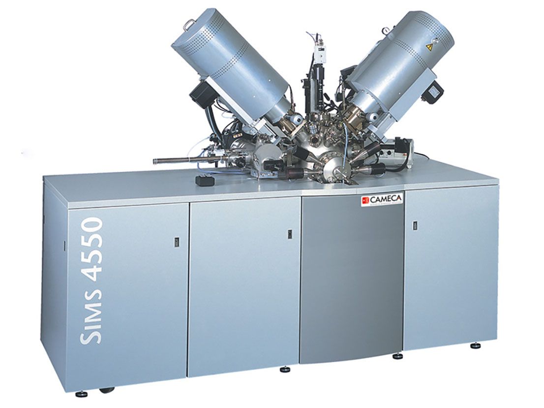
    Secondary Ion Mass Spectrometry (SIMS) is a highly sensitive technique used to analyze the composition of solid surfaces and thin films. It works by bombarding the sample with a focused ion beam, which sputters atoms and molecules from the surface. Some of these become ionized (secondary ions) and are analyzed by a mass spectrometer to determine their mass-to-charge ratio.

    SIMS is especially useful for depth profiling and trace element detection, with applications in semiconductors, materials science, geology, and more. It can detect almost all elements, including light ones like hydrogen, down to very low concentrations (ppb level).

    Principle

    Principle

    Working Principle of Static SIMS

    Static Secondary Ion Mass Spectrometry (Static SIMS) focuses on analyzing the very top surface layer of a sample—typically the outermost 1 to 3 atomic layers. In this mode, the primary ion beam has a low energy, usually around 100 eV, and only a very small number of atoms are sputtered from the surface during analysis. This ensures that the surface remains largely intact, making Static SIMS a non-destructive technique ideal for surface chemistry and molecular studies. The extremely low sputter rate allows detailed characterization of surface composition without altering the original structure.

    Working Principle of Dynamic SIMS

    Dynamic Secondary Ion Mass Spectrometry (Dynamic SIMS) is designed for depth profiling, revealing how elemental composition varies below the surface. In this mode, the primary ion beam has a higher energy, typically between 1–10 keV, and it sputters a significant amount of material from the surface with each pass. This leads to gradual erosion of the sample surface, allowing deeper layers to be exposed and analyzed. The higher sputter rate enables rapid acquisition of depth information, making Dynamic SIMS well-suited for quantitative analysis of layered structures, dopants, and trace elements in materials.

    • SIMS is primarily used for static surface analysis, while D-SIMS is suitable for dynamic analysis, providing deeper insights into layered structures.

    • A variety of materials can be analyzed, including semiconductors, metals, polymers, and ceramics, particularly suitable for thin films and composite materials.

    • SIMS and D-SIMS can detect elements at parts-per-million (ppm) levels, making them suitable for tracing trace components.

    • The typical testing thickness is generally within 5 µm but should not exceed 10 µm to ensure accuracy and reliability.

    Depth profile for Electronic materials

    Depth profile for Electronic materials

    Applicable Material Types

    • Semiconductors: Silicon, gallium arsenide, silicon carbide, etc., commonly used in integrated circuits and optoelectronic devices.
    • Thin Films & Multilayers: Metal oxides, nitrides, dielectric films, and multilayer structures used in microelectronics and coatings.
    • Metals & Alloys: Copper, aluminum, titanium, stainless steel, and high-temperature alloys, especially for trace impurity and surface treatment analysis.
    • Ceramics & Oxides: Alumina, zirconia, silicon nitride, often used in wear-resistant coatings, fuel cells, and electronic ceramics.
    • Glass & Optical Materials: Borosilicate glass, fused silica, used in photonics, lenses, and solar devices.
    • Battery Materials: Lithium-based cathode/anode materials, solid electrolytes, used in lithium-ion and solid-state batteries.
    Depth profile for Electronic materials

    Depth profile for Electronic materials

    Industrial Application

    • Semiconductor Industry:For precise depth profiling of dopants, contamination detection, and multilayer interface analysis in ICs and MEMS fabrication.
    • Materials Science & Engineering:Used to study diffusion, segregation, and interfacial phenomena in metals, ceramics, and advanced functional materials.
    • Geology & Earth Sciences:Applied in isotope ratio analysis and trace element distribution in rocks and minerals for geochronology and environmental studies.
    • Aerospace & Defense:Used to characterize protective coatings, detect trace contaminants, and analyze surface composition changes due to environmental exposure.

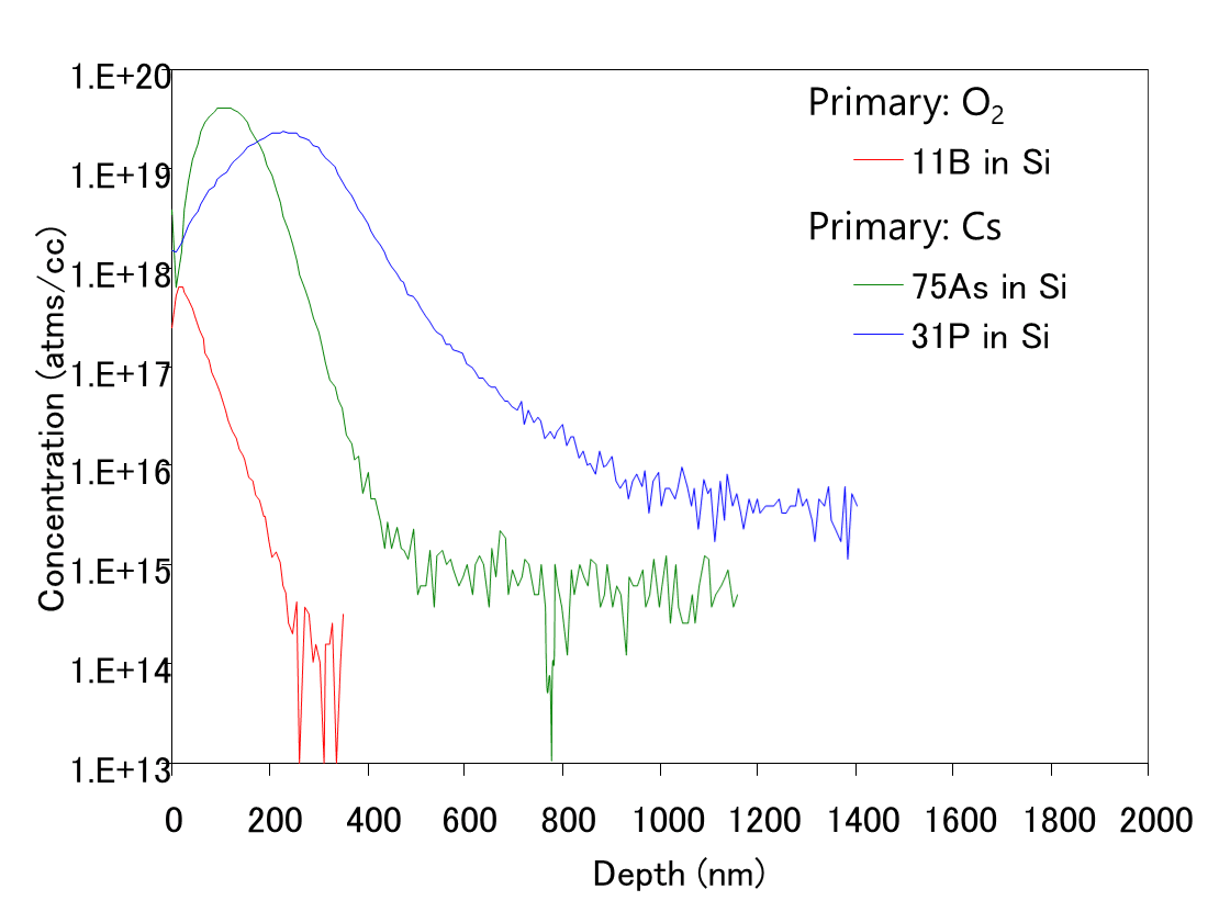
    1. Caption: D-SIMS Doping depth analysis.
    1649750778279_图片111.png

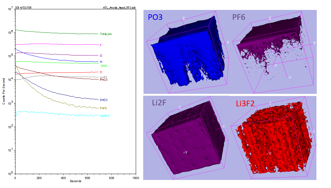
    2. Caption: TOF-SIMS Depth Profiling & Data Analysis.
    1637207482969_mceclip4.png

    CategoryTOF-SIMS Sample RequirementsD-SIMS Sample Requirements
    Applicable Sample TypesPowder, bulk solids, and flat-surfaced materials. Suitable for surface chemical analysis and mapping.Solid thin films or flat, smooth surfaces such as substrates or deposited layers. Used for depth profiling and quantitative analysis.
    Sample Size- Bulk: ≤ 1.1 cm (L/W), thickness ≤ 5 mm- Powder: ≥ 50 mg- Size: 5–10 mm- Thickness: ≤ 1 mm- Clearly mark the test surface
    Sample Preparation- Powders must be dry, dehydrated, and vacuum sealed- Moisture-sensitive or oxidizing samples require pre-arranged testing and vacuum sealing- Avoid sticky plastic bags, tapes, or adhesive films- Store samples in vacuum- Powders, packaged, or structured samples require additional sample preparation
    Vacuum StabilityMust be stable under ultra-high vacuum (UHV) and free from corrosive/volatile emissionsSame as TOF-SIMS: must be UHV-compatible and chemically stable
    Analysis Mode- Mainly used for surface mass spectrometry and 2D mapping- Not used for depth profiling- Used for depth profiling and trace analysis- Quantification possible with suitable standards (e.g., B, P, As in silicon)
    Analysis DepthTop 1–2 nm of the surface; extremely surface-sensitiveTypical analysis depth: <5 µm, max ≤10 µm
    Analysis AreaFlexible; typically small areas (tens to hundreds of µm²)Standard areas: 100 × 100 µm², 200 × 200 µm², 300 × 300 µm²Larger areas = slower sputtering

    Secondary Ion Mass Spectrometry (SIMS) is a surface analysis technique that uses a focused ion beam to ablate the sample layer by layer. As material is sputtered from the surface, secondary ions are emitted and analyzed by a mass spectrometer. This enables precise chemical characterization of the sample as a function of depth, making SIMS especially useful for generating depth profiles of elemental and isotopic composition.