
info@universallab.org
WhatsApp: +41762172997

Price may vary based on selected options
Delivery time: 1 ~ 2 weeks

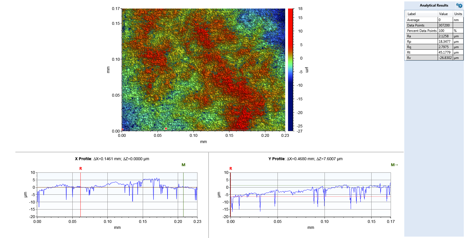
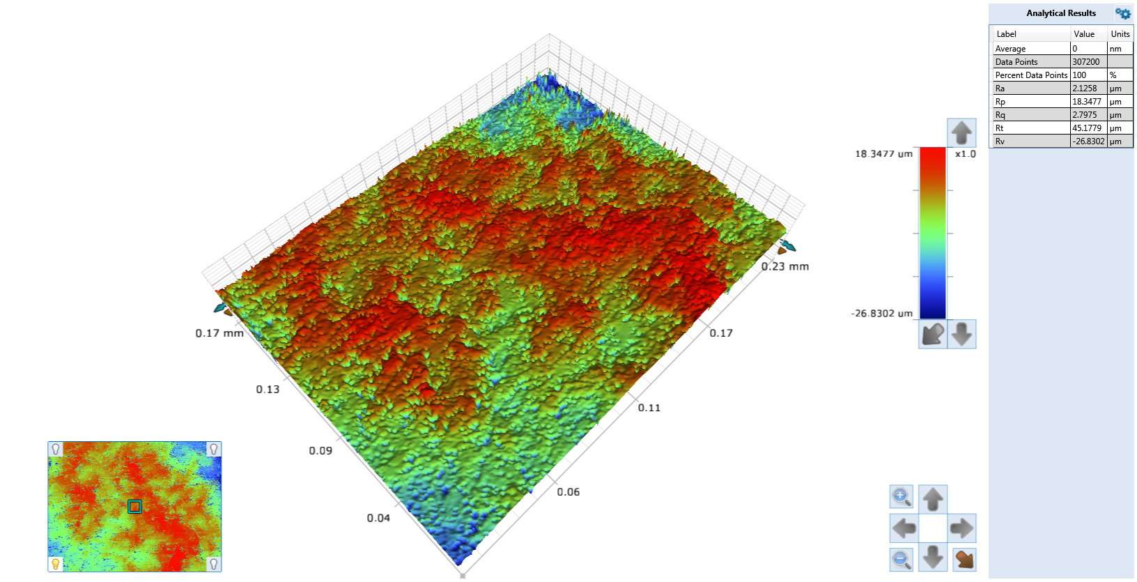
Stylus Profilometer is a precision surface measurement instrument used to evaluate surface roughness, waviness, step heights, and other fine surface profiles. By dragging a sharp diamond-tipped stylus across the sample surface, it records vertical displacement to generate a detailed 2D or 3D surface map.
This technique is widely used in semiconductor manufacturing, precision engineering, thin-film analysis, and materials research for assessing surface quality, process control, and functional performance.

The stylus profilometer works on the principle of mechanical contact measurement:
This contact method allows very high vertical resolution (down to nanometers) and is widely considered a standard reference technique.

Typically up to ~100 μm vertical features, depending on stylus range.
For most hard surfaces, no. For soft or delicate materials, we use minimum force or recommend non-contact methods.
Yes, down to ~10 nm depending on material contrast and tip selection.
Typically up to tens of millimeters in length; area scans are limited and may require stitching.

Stylus Profilometer measurement applies to a wide range of materials and components, including:
To ensure accurate measurements, samples must meet the following conditions:
| Feature | Description |
|---|---|
| Vertical resolution | Excellent (nanometer-level) |
| Lateral resolution | Limited by tip radius (typically micrometers) |
| Measurement speed | Moderate; slower than optical methods |
| Surface compatibility | Works on reflective, transparent, or opaque materials |
| Main advantage | Direct physical measurement, high accuracy on roughness |
| Limitations | Potential sample damage on soft materials; limited to line or small area scans |
| Technique | Contact/Non-contact | Vertical Resolution | Lateral Resolution | Speed | Typical Applications |
|---|---|---|---|---|---|
| Stylus Profilometer | Contact | Nanometer-level | Micrometer (tip limited) | Moderate | Roughness, step height, wear, defect analysis |
| Optical Profilometer | Non-contact | ~1 nm (depends on system) | Sub-micron (diffraction limited) | Fast | Soft surfaces, delicate films, transparent materials |
| AFM (Atomic Force Microscopy) | Contact (nanoscale) | Sub-nanometer | Nanometer | Slow (small area) | Nanoscale surface structures, high-res mapping |
| SEM (with surface analysis) | Non-contact (electron beam) | Sub-nanometer (vertical) | Nanometer | Moderate to slow | Micro/nano-scale topography, morphology |
Stylus Profilometer is a precision surface measurement instrument used to evaluate surface roughness, waviness, step heights, and other fine surface profiles. By dragging a sharp diamond-tipped stylus across the sample surface, it records vertical displacement to generate a detailed 2D or 3D surface map.
This technique is widely used in semiconductor manufacturing, precision engineering, thin-film analysis, and materials research for assessing surface quality, process control, and functional performance.